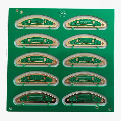
Heavy Copper PCBDate: 2022-12-12

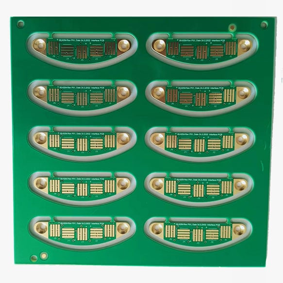
- PRODUCT DETAIL
- TECHNICAL SPECIFICATIONS
Design Considerations for Thick-copper Boards
Thickness and width of copper
PCB designers calculate the amount of current required and design their hefty copper boards accordingly. This includes determining the appropriate copper thickness, width, and maximum temperature rise that the circuit board can withstand. The quantity of heat generated by a hefty copper board is related to the amount of current it carries.
How to select the correct copper thickness?
As previously stated, the current traveling through the conductor determines the copper thickness. A trace-width calculator can be used to determine the thickness of the board. It can compute three parameters: trace width, current capacity, and temperature rise.
Current carrying capacity
As current flows through a copper trace, its resistance heats it up inadvertently. The power generated by the local heat transition is dissipated into the atmosphere via conduction and convection. The maximum current that the trace may carry before reaching the allowable temperature rise of roughly 30°C must be calculated by the designer. The industry standard is that the inner layers can only support 50% of the current-carrying capacity of the exposed traces.
Substrate substance
Another element to consider when constructing hefty copper boards is the PCB substrate. The substrate materials range from standard FR-4 with an operating temperature of 130°C to advanced materials with extremely high glass transition temperatures (Tg). Because a large current can induce cracks and layer separation, the Tg of the copper and substrate material is crucial.
Thermal expansion coefficient (CTE)
The rate of expansion of a PCB material when it heats up is defined as its coefficient of thermal expansion (CTE). It is measured in parts per million (ppm) expanded for every degree Celsius heated. CTE between copper and the substrate material is also essential because thermal stress caused by large currents through traces can cause fractures to grow, eventually leading to board failure.
Electroplating can be used to increase the surface thickness of a circuit board. It decreases the resistance of copper traces by improving heat conduction. Fabricators utilize electroplating to reduce the heat resistance of PTHs. Resistance reduction aids in the effective dissipation of heat via heat transfer mechanisms such as conduction, convection, and radiation.
Advantages of Thick Copper PCB
Heavy copper PCB is the preferred choice for several unusual circumstances and high-end applications due to its unique advantages. We’ll go over some of its highlights below:
● Ultra-high mechanical strength: The printed circuit board has ultra-high mechanical strength after thick copper is put to the circuit and vias of the board. Increases the weather resistance of the circuit board and the electrical system. It has a high melting point and is not brittle at low temperatures, making it suitable for use in hot melt welding procedures such as oxygen blowing. Copper weight PCB forms a strong, non-toxic passivation protective layer even in severely corrosive air situations.
● Excellent weather resistance: The hefty copper PCB board allows for the use of a variety of dielectric materials. It can assure the stability of the circuit transmission signal under high-temperature or extreme-environment conditions. Special dielectric materials improve the board’s overall weather resilience.
● Thermal Management: As current technology advances, PCBs get more and more sophisticated. The problem of thermal management is exacerbated by the high density of current. Excessive heat can disrupt the normal operation of electrical equipment and potentially cause it to fail. The thick copper PCB board may provide better heat dissipation. Heatsink matching and copper plating via holes can significantly reduce board heat.
● Outstanding current conduction: The heavy copper printed circuit board is an excellent current conductor in the functioning of electronic equipment. It can be attached to various boards to convey electricity.
● Diversity: Its conductive materials, substrate materials, manufacturing technique, and application domains differ from normal PCBs. The plating of thick copper circuits enables heavy copper PCB makers to increase copper weight through sidewalls and plated holes, allowing them to lower layer counts and footprints.
● Extendability: Thick copper PCB offers the best elongation performance and is not temperature limited.
● High performance: Thick-copper plating incorporates high-current and control circuits, allowing for high density with simple board architectures.
Difference Between Standard PCB and Heavy Copper PCB
1. Standard PCBs are made fast using copper etching and plating methods. The boards are coated in order to increase the copper thickness of the traces and planes. In addition, 1oz of copper is utilized in conventional PCBs.
Heavy copper PCBs, on the other hand, are manufactured using several ways, and the amount of copper utilized is greater than 3oz.
2. CNC cutting, copper etching, and plating processes are used with typical printed circuit boards. Heavy copper PCBs, on the other hand, are created using various etching and step plating techniques.
3. Standard printed circuit boards do lighter tasks, whereas heavy copper printed circuit boards handle heavier tasks. Furthermore, ordinary PCBs conduct a smaller current, whereas hefty PCBs conduct a high current.
Applications of Heavy Copper PCB
A heavy copper printed circuit board has a higher copper weight, which, when combined with the appropriate high-temperature laminate material and thicker through-hole copper plating, can transform a flimsy board into a long-lasting and dependable wiring platform. Heavy copper conductors can significantly increase the overall thickness of the PCB. During the circuit design stage, the copper thickness should always be taken into account. The breadth and thickness of the heavy copper determine the current-carrying capability.
Heavy copper Printed Circuit Boards are utilized for a variety of applications, including planar transformers, heat dissipation, high power distribution, power converters, and so on. Heavy copper-clad boards are in high demand in computer, automotive, military, and industrial applications. Heavy copper printed circuit boards are also utilized in the following applications:
● Power sources and converters
● Power distribution
● Welding apparatus
● The automobile industry
● Solar panel manufacturers, etc.
Thick copper Printed Circuit Boards are increasingly being used in power electrical devices and power supply systems. This one-of-a-kind heavy copper PCB has a completed copper weight of more than 4oz (140m), as opposed to the 1oz (35m) or 2oz (70m) copper weight seen in normal designs.
Why Choose Thick Copper PCB for Your Applications?
In applications needing high power or current, heavy copper PCBs can provide various advantages. The following are some of the characteristics that contribute to the popularity and widespread acceptance of thick copper PCBs.
● Can endure repeated exposure to high current.
● High tolerance capacity.
● High resistance to thermal stresses.
● Improved current conductivity.
● Can withstand repeated thermal cycling.
● Copper layers result in smaller PCB sizes.
● Lower failure rates.
● Strengthened connector site.
● Reduced production expenses.
● Superior mechanical strength at the connector and PTH holes.
UnitePCB Capabilities in Thick Copper PCB Manufacturing
UnitePCB has the production experience, the proper personnel, and the facilities to handle difficult heavy copper PCB fabrication. Whatever your requirements are, we rigorously incorporate them into the design, assisting customers in meeting their efficiency and profitability targets. We have the following skills as an experienced thick copper PCB manufacturing.
| Feature | Capability |
| Material | FR-4, Metal Core substrate |
| Min. Track/Spacing | For External layers: 4oz Cu 9mil/9mil,5oz Cu 11mil/11mil 6oz Cu 13mil/13mil,12oz Cu 20mil/32mil For Internal layers: 4oz Cu 8mil/12mil,5oz Cu 10mil/14mil 6oz Cu 12mil/16mil,12oz Cu 20mil/32mil |
| Min. Hole Size | 0.15MM |
| Max Outer Layer Copper Weight (Finished) | 20oz |
| Max Inner Layer Copper Weight | 15oz |
| Board Thickness | 0.5-6mm |
| Surface Finishing | Immersion gold, Immersion Silver, OSP, Hard Gold, Enepig, HASL lead free |
| Solder Mask | Green, Red, Yellow, Blue, White, Black, Purple, Matte Black, Matte green |
| Silkscreen | Green,Yellow, White, Black |
| Via Process | Tenting Vias, Plugged Vias, Vias not covered |
| Testing | Fly Probe Testing (Free) and A.O.I. testing |
| Delivery Time | 3-10 Working days |
Video of Our Heavy Copper PCB Products
Video of our PCB production and processing
Get a Quote for Custom Thick Copper PCB
UnitePCB provides the technology, deep engineering experience, and knowledge to assist you in correctly designing and building a heavy copper PCB from the outset. We can create a PCB with up to 6 ounces of copper for the outer layers and up to 4 ounces of copper for the interior layers using our revolutionary capabilities. If you have any queries regarding how much copper you’ll need for your project, please contact us and we’ll get back to you as soon as possible.
To offer you with a price within 24 hours, we use a well-organized methodology and the appropriate software. Our engineering staff will examine the data and give us with a thorough document when you upload your information, including any fabrication drawings or schematics, so we can take a closer look at your heavy copper PCB project.
TECHNICAL SPECIFICATIONS
| Feature | Parameters |
| Maximum Number of Layers | 60 |
| Materieal | Laminate-FR-4 (All Tg Ranges),Teflon,Ceramic |
| Finished Thickness | 0.020"-0.275" |
| Soldermask | Green,Blue,Red,Black,Clear and White Solder Masks&Legend Inks |
| Minimum Soldermask Clearance | 6 mils |
| Minimum Solder Dam Width | 5.5 mils |
| Surface Treatment | Hot Air Solder Leveling(HASL) Immersion Gold (ENIG)&Immersion Silver |
| Degree of Difficulty | Blind & Buried Vias |
| Minimum Drill Bit Hole Size | 0.012" |
| Minimum Holes Size | 0.008" +0.005"/-0.008" |
| Technical Feature | 90Ω & 100Ω Differential impedance, thick cooper |
| Maximum Hole Aspect Ratio =10:1 | |
| Maximum Copper Weight | 6 oz.(UL Approved) |
| Controlled Impedance | +/- 10% |
| Minimum Silkscreen Line Width | 8 mils |
 Manufacturer")


