High-density Interconnect PCBDate: 2022-12-27
- PRODUCT DETAIL
- TECHNICAL SPECIFICATIONS
High-density Interconnect PCB Manufacturing
You are correct if you believe that manufacturing HDI PCBs necessitates special equipment or extra time, because assembling these high-quality boards necessitates a variety of processes and special equipment. Drilling small microvias requires laser drilling technology, which allows for the use of other techniques on the board. Because HDI PCBs are multilayer boards with densely wired layers, the lamination process is also more complex.
Design Considerations for HDI PCBs
The manufacturing process for HDI PCBs is typically distinct from that of other PCB types. Here’s everything you need to know about HDI board production, as well as some design considerations to keep in mind throughout the manufacturing process.
● Sequential lamination: During the lamination process, heat and pressure are used to bond the PCB core or cores to the copper and prepreg layers of the multilayer PCB. The amount of heat and pressure needed varies depending on the board. The PCB manufacturer drills the holes after the lamination phase is completed. HDI boards, unlike other types of PCBs, go through this process multiple times. During the drilling process, these successive laminations help to prevent displacement and breakage.
● Overfill type: Always match the overfill type to your specific application and PCB requirements. Electrochemical plating, silver fill, copper fill, conductive epoxy, and non-conductive epoxy are some of the overfill materials we frequently use. A non-conductive epoxy is the most common type of overfill. The fill must allow for blind, buried, or drilled microvias and standard vias to be plated and hidden beneath the SMT pads. To ensure that the drilling process is completed correctly each time, we frequently use multiple drilling cycles at precisely controlled depths. This level of control necessitates the use of specialized equipment as well as longer development times.
● HDI Structures: HDI PCBs are available in a variety of layout options. 1-n-1 and 2-n-2 PCBs are two of the most common. Because 1-n-1 PCBs only have one high-density interconnect layer, they are the “simplest” type of HDI PCB. Each side of the core must be sequentially laminated. Microvias can be staggered or stacked across layers on 2-n-2 PCBs, which have two HDI layers.
● Laser Drilling Technology: Laser drilling is typically used to create laser microvias in any layer HDI design. These drills generate laser light with a diameter of up to 20 microns and can effortlessly cut through metal and glass to create very small but clean holes. Even smaller holes can be obtained by using materials with a low dielectric constant, such as homogeneous glass.
What To Look For in HDI Assembly?
Because of the PCB’s smaller and more compact form factor, placing components on the PCB requires greater precision than traditional PCB designs. Special soldering techniques and additional steps in the assembly and rework (repair) processes are required for bga and flip chip.
Differences Between Standard Boards and HDI PCBs
Through-holes are commonly used on standard printed circuit boards to achieve high stray capacitance and large impedance discontinuities. They improve average signal integrity performance in layman’s terms. To reduce stray inductance and capacitance, HDI boards use buried and blind vias. As a result, signal integrity performance is excellent.
Other notable distinctions between standard and HDI boards include.
● HDI PCBs have a higher component density per square inch than standard PCBs.
● Mechanical drilling is used on standard boards, whereas direct laser drilling is used on HDI PCBs.
● Standard PCBs are heavier and larger, whereas HDI PCBs are lighter and smaller, but perform better.
● Standard printed circuit boards have many layers, whereas HDI printed circuit boards have few layers.
● A standard PCB has compatibility issues when paired with a low pitch package, whereas HDI boards work well with both low pitch and high pitch packages.
HDI Features and Benefits
The significantly higher package density is the most common reason for using HDI technology. The extra space created by finer track structures and microvias can be used for components and landing surfaces. Furthermore, overall space is reduced, resulting in smaller board sizes and fewer layers required.
● Because HDI PCBs can be mounted on both sides of the board, designers can integrate more components onto smaller boards.
● Cuts down on power consumption, extending the battery life of handheld devices and other battery-powered devices.
● Rougher for increased strength and less perforation.
● Reduces thermal degradation, extending device life.
● Enables more efficient and dense transfers and calculations in smaller areas, resulting in smaller end-user products like smartphones, aerospace devices, military equipment, and medical devices.
● The long-term viability of dense BGA and QFP packages in PCB designs.
● If you use smaller BGA and QFP packages in your designs and applications, HDI PCBs can provide higher transfer reliability when your PCB designs are mass-produced. HDI PCBs can support denser BGA and QFP packages than previous PCB technologies.
Application of HDI Printed Circuit Boards
Many of today’s advanced technologies rely on HDI technology. Miniaturization of electronic components, including printed circuit boards (PCBs), enables manufacturers to produce smaller, more cost-effective devices without sacrificing performance or reliability.
HDI PCBs are widely used to reduce product weight and overall size while also improving device electrical performance. Cell phones, touch-screen devices, laptops, digital cameras, and 4G network communications all use high-density PCBs. HDI PCBs are also widely used in medical devices and various electronic aircraft components.
Our HDI PCB Manufacturing Capability
Our laser direct imaging (LDI) capabilities ensure precise alignment and examination of all internal layers. UnitePCB’s common advanced HDI PCB manufacturing capabilities are listed in the table below.
| Feature | Capacity |
| Quality Guarantee | Standard IPC Class 2 |
| Material | Tg 140C standard FR4, Tg150C FR4, High Tg 170C FR4, FR4, and other custom materials. |
| Number of Layers | 4-36 layers |
| Board Thickness | 0.4mm – 6.0mm |
| Copper weight (Finished) | 0.5oz – 14oz |
| Min Track / Spacing | 2.5-8 mil |
| Solder Mask Color | Green, White, Blue, Black, Red, Yellow |
| Silkscreen Color | White, Black, Yellow, Red, Blue |
| Surface Finishing | Immersion gold, Plated Gold, OSP, ENIG, Immersion Silver |
| Min Annular Ring | 4mil, 3mil – laser drill |
| Min Drilling Hole Diameter | 6mil, 4mil – laser drill |
| Max blind/buried vias exponents | Staggered vias for three interconnected layers, and staggered vias for four interconnected layers. |
| Other Techniques | Flex-rigid combination Via In Pad Buried Capacitor (only for Prototype PCB total area ≤1m²). 1+N+1: Blind vias -4 layers+ 2+N+2: Blind/Buried staggered vias -6 layers+ 2+N+2: Blind/Buried stacked vias -6 layers+ 3+N+3: Blind/Buried staggered vias -8 layers+ 3+N+3: Blind/Buried stacked vias-8 layers+4+N+4: Blind/Buried stacked vias-10 layers+ |
| Build Time | 2days-5 weeks |
The following are some of HDI’s exceptional manufacturing capabilities.
● Microvia sizes as small as 25 microns
● Line and width spacing are reduced to 19 microns.
● A copper thickness of as little as 5 microns
● Microvia pad dimensions as small as +150 micron through-hole diameter
● Aspect ratio of blind microvia plating (depth to diameter): 1.2:1.
● Core dielectric thickness of 12 microns or less
● Construction of blind buried holes using sequential build technology
● Copper through-hole filling that is readily available
Video of Our HDI PCB Products
Video of Our HDI PCB Production and Processing
Why Choose UnitePCB’s HDI PCB Manufacturing Services?
We have a solid reputation in the market due to our years of experience in HDI PCB manufacturing. Our top priority is to provide you with a high-quality product. Our company’s mission is to provide excellent products to our customers. We also offer custom high density interconnect printed circuit boards. Our in-house design team will work with you several times to create a product that meets all of your specifications. Furthermore, our quality control team ensures that the finished product is of the highest quality.
TECHNICAL SPECIFICATIONS
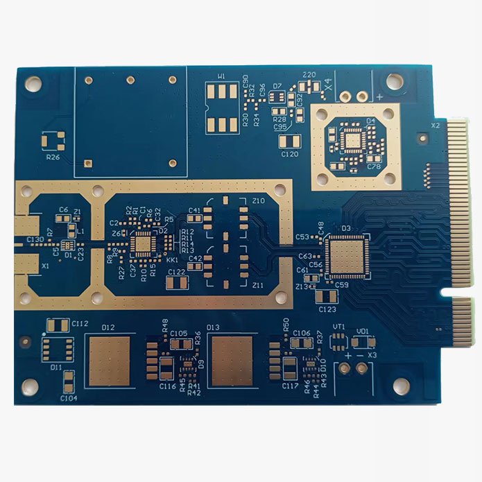
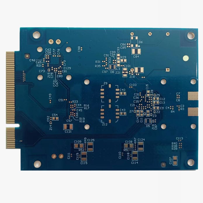
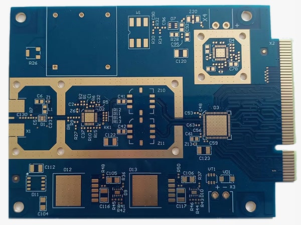
10 Layer HDI PCB multilayer S1000-2M,TG180 PCB (1+8+1)
| Feature | Parameters |
| Material | S1000-2M, TG180° |
| Layer Count | 10 (blind & buried vias, high speed) |
| Finished Thickness | 2.0 mm+/-10% |
| Finished Copper | inner: 35 um, outer: 70 um |
| Surface Finish | ENIG (Immersion gold: 3μ") |
| Minimum trace/space | 3mil/3mil |
| Min. Hole Size | 0.1mm |
| Min NC Drilling | 0.203mm |
| Special Hole Tolerances | |
| Resin Filled & Capped Vias | yes |
| Impedance Control | yes (differential 90 & 100 ohm / 3 impedance control values) |
| Technical Feature | 90Ω & 100Ω Differential impedance, thick cooper |
 Manufacturer")


